Clocks
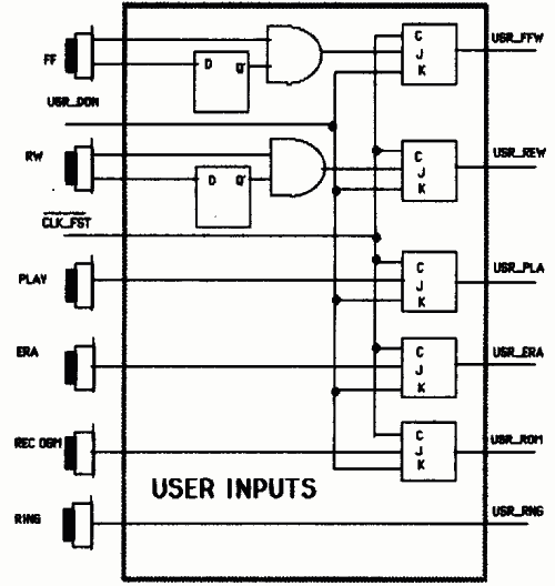
User Inputs
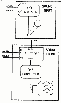
Analog Interface
Controller
Address Controller
Data Storage
Memory Registers
The Beep Generator In All Its Glorious Splendor
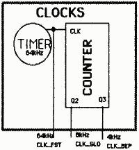
In our project, one of the major concerns was clocking. Most of SPAM is very fast, the very noticeable exception being the ADC, which takes on the order of microseconds to do its thing. If we clocked SPAM slow enough for the ADC not to be overwhelmed, we would have a slow machine. What we ended up doing was hooking our clock up to a counter, using said counter as a bank of toggle flip flops. In this way, we were able to clock the controller at a speed which was still slow, but which would give it a chance to handle instructions between ADC enables. The ADC's clock came out of the counter, and was 1/8 as fast as the standard clock. We also used this ADC clock as clock input for our speaker latch, thus helping to ensure that sound would be output at the same speed input.
We used a 555 timer to output a 64 Khz square wave. A counter was wired so that it would increment every clock tick. The output from the 555 was the 'clock' used by most of our chips, and was called the fast clock or CLK_FST. The counter generated the ADC clock of 8Khz. As mentioned, this clock was used for the ADC and the DAC latch. Identified as the slow clock or CLK_SLO it was also fed to the controller as an input to aid with synchronization. Other clock signals were the beep clock (called CLK_BEP), used to generate a wave slow enough to produce a tone when sampled by the DAC.
Not shown in this block diagram is the inverse clock, which was used as a kludgy fix to some J/K flip flops that gave us grief in the user inputs block. The 64 KHz clock used a 555 timer with a 1kOhm resistor between pins 6&7, a 330 Ohm resistor between pins 7&8, and a .01uFarad Cap. from pin 6 to ground. This results in a period of (0.7)*(2000+330)=16.3usec, for a 61KHz frequency.
And boy, did user inputs ever give us grief. The problem was that humans are slow. They stick their big, fat fingers on a button, and keep the poor little dear pressed down so long... sometimes even seconds at a time. We quickly realized that if we just gave the button outputs as inputs to the controller without doing anything to them we'd run into all sorts of problems. People rewinding 500 times or so, because the controller would have time to skip over a lot of messages before most people could free their fingers.
We figured out what we had to worry about for each button.
To catch the forward edges of Fast Forward and Rewind, we used single throw double pole buttons, debounced. The button outputs were sent to two places - a D flip flop and an AND gate. The inverse output of the D f/f acts as the other input to the AND gate (I'm not saying this well - just look at the picture). Since we hooked up the inverse output of the flip flop to the AND gate, the AND's output only goes high when the input presently high but was low one tick ago - that is, on a forward edge. The outputs of these edge catchers was fed into yet more J/K flip flops in the same way as Erase. Unfortunately, when we actually built this circuitry, the timing of the latches was just a little bit off, and the AND's output wasn't staying high quite long enough to get latched by the J/K (though our CAD program thought it would be OK). We wanted to just "jiggle the clock a little." We tried inverting the clock input to the J/K flip flops. Everything worked like a charm after that.
The outputs of this block, all going to the controller were USR_FFW, USR_REW, USR_PLA, USR_ERA, USR_ROM, and USR_RNG, corresponding to Fast-Forward, Rewind, Play, Erase, Record Outgoing Message, and Ring, respectively.
This was the scariest part of SPAM. When things went wrong, it was hard to tell just what was responsible. And since the most mistakes resulted in a rather uninformative silence, it was hard to even tell various recurring problems apart. Not to mention that this was some expensive equipment.
The microphone we ended up using was a professional model on loan from the rock band Megabrooce. The speaker we demoed with was borrowed from a good friend (see credits). If we destroyed either, we were out some serious cash.
As if that wasn't enough, our most expensive chip, the $14.00 ADC was part of this block and it kept getting hot. Like blistering.
Fortunately, we had been given plans for the DAC from on high. Our decision to use a shift register to latch the data was a simple one of availability - we never use it to shift, and it in fact is wired so that it can't. It was just a chip we didn't have any other use for which could handle the job at hand. Besides, its chip was smaller than those for regular latches.
Strangely enough, though we were using the standard plans provided for wiring up the output, we seemed to have a lot more trouble with our sound than the rest of the class when using an ordinary speaker, which seemed to load our output to a surprising degree, causing the output waveform to be clipped. When we used an independently powered speaker, however, we managed to create some truly superior sound. Not to mention loud.
It is clocked using the slow (8Khz) clock, and the controller output DAC_ENA (D/A converter enable) turns it on and off. It gets data input from the data bus. Since we were using a non-standard microphone (after getting tired of screaming at the expected el-cheapo condenser mike units), we couldn't use the provided input circuitry, either. The problem is that the moving coil mike was not a variable capacitor, but a variable voltage source. It generated a signal centered at 0V, with peak to peak values in the millivolts. We then biased the signal by a very small voltage to bring it fully into the positive voltage range. Then, we amplified this whole signal, DC bias and all, to get a clean signal ranging from about 3V to about 3.8V. We then adjusted the ADC reference voltages accordingly.
The ADC chip is clocked by CLK_SLO (8KHz), and enabled by the controller output ADC_ENA (A/D Converter Enable) determines whether the output will be put onto the data bus or just left as Tri-State®.
HIGH ROM PIN: H7 H6 H5 H4 H3 H2 H1 H0 L7 L6 L5 L4 L3 L2 L1 L0 Table illustrating the format of a controller signal.
On a D0, the data |
In trying to strike the balance between using more hardware or more sophisticated software, the place where we found ourselves making the most difficult tradeoffs was the controller. If we wanted powerful software to make up for a lack of hardware, we would want to jazz up our microcontroller to allow cool programming techniques. We considered but ended up rejecting implementing subroutine calls. Since we were going to be using an assembler capable of expanding macros, it wasn't going to be much trouble to include blocks of code multiple times, and it wasn't looking as if we were going to be taking up much space, even if we were to repeat a lot of code.
One spiffy gimmick we did end up implementing was the branch on inverse command, which allowed for some more intuitive code.
Our microcontroller design was pretty much a copy of that presented by Wayne in his microcontroller lecture. There are basically 4 parts: ROM, counter, multiplexer, and latch. The ROM supplies instructions which govern the behavior of the other components. The multiplexer is used to select a controller input for branch statements. The counter is used to keep track of the ROM address. Normally, the counter just increments, but on a branch statement when the multiplexer output is low, the counter loads an address supplied by ROM. The latch inputs data supplied by the ROM when the ROM sets input enable low.
Put it all together and you've got a controller: The counters supply the ROM with an address. If the high bit of the contents of that address is a 0, the latch latches the rest of the contents, and passes them on to the rest of SPAM. If, on the other hand, the high bit of is high, the latch just keeps on outputting what it was last clock tick and the output of the multiplexer is compared to the second highest bit coming out of the ROM. If they're equal, then the load on the counters is enabled.
In other words, our controller is a lot like everyone elses'.
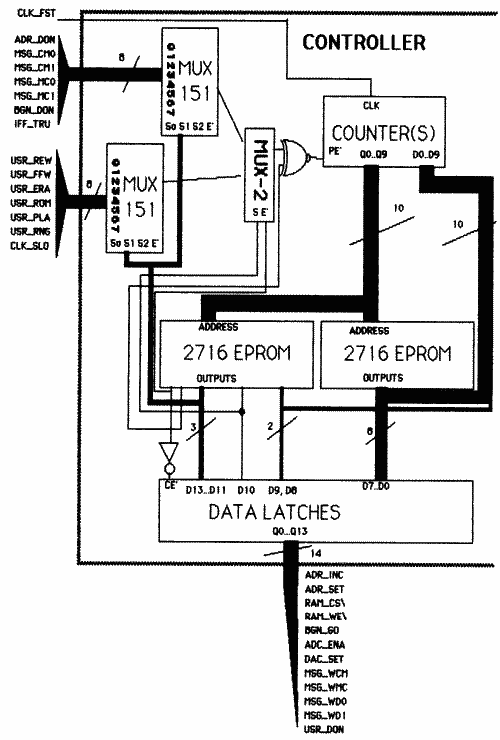
Our ROM consisted of 2 EPROMs, known as High and Low or Orange and Yellow. We used '377 latches, since they were latches we had on hand with the necessary input enable. Our counter consisted of 2 cascaded 161's, and again our choice of chip was based on what we had on hand. For our multiplexers, by once again working with chips which were available we saved ourselves a bit of worry. Instead of using an XOR gate to determine whether multiplexer input was equal to the 2nd highest bit of ROM, we decided to use the 2nd highest bit as another multiplexer selector. This presented no extra hardware cost, since the second level mux would have been needed anyway. We ended up with our inputs going into 2 151 multiplexers, choosing between their outputs with a 153 multiplexer.
Inputs to the controller were the fast clock (CLK_FST), RESET (which cleared the counters, effectively starting the controller over at instruction 0), and the branch conditions: USR_REW, USR_FFW, USR_ERA, USR_ROM, USR_PLA, USR_RNG (User Inputs), CLK_SLO(the 8KHz clock), ADR_DON (the end-of-message indicator), MSG_CM0, MSG_CM1, MSG_MC0, and, MSG_MC1 (the contents of the message registers).
Another condition was called IFF_TRU; it was hardwired high, and was included for unconditional branches. The controller outputs were ADR_INC, ADR_SET (controls for the address controller (does that make them meta controls (is that a meta-parenthetical statement?))), RAM_CS\, RAM_WE\ (controls for the data memory), BGN_BP\, ADC_EN\, DAC_ENA (enables for the beep generator, mike, and speaker), MSG_WCM, MSG_CM\, MSG_MC\, MSG_WD0, MSG_WD1 (message register controls), USR_DON (clears out user inputs).
In spite of the fact that we were willing to make our controller more complicated to make our hardware simpler, we were able to get away with using a small number of output signals so that we didn't have to do any decoding. And few enough inputs so that we only had to use two and one half (2 1/2) multiplexers. Sweet huh? All this and branch on zero, too.
We didn't implement subroutines, but when we looked at the tradeoffs involved - lots more controller details, with registers to store addresses, multiplexers to choose between loadable addresses... Much better that we have a controller which doesn't even fill half a board Also, most of our microcode routines all ended up by returning to the main event loop.
When we actually built the thing, we used a row of staples to provide a nice, linear set of holes on the board corresponding to ROM outputs.This made finding and connecting to the outputs easier than if that had been scattered around the outputs of a latch, and since they were exposed, these staples were easily read by a logic probe, and were a great boon to SPAM's testability.
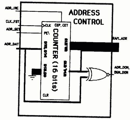
One thing we knew we were going to have to deal with was a lot of data. Storing 8 seconds worth of noise (also known as sound) with a sampling rate of 8KHz at 4 bits resolution well that's 8x8000x4 is... well, that's a lot of memory. Basically, what we needed was a whole mess of counters that could do a nice job of coming up with nice sequences of addresses for us to hand the RAMs when we wanted to store or fetch noise. It was clocked by the fast clock, and was controlled by the ADR_INC and ADR_ST\ controller outputs. The first would increment the counters. The second would make them load an address.
The idea was that when beginning to record or play back a message, to load the counters with an address supplied by ADR_DAT (the output of the Current Message register), and then play or record to addresses supplied by the counter as it was repeatedly incremented. When either of the high bits of the counter disagreed with their corresponding bit of ADR_DAT (XOR=1), that meant that the counter had reached territory set aside for another message, and so it sent back the signal ADR_DON (address Done), so the controller would know that it was done with that message. We ended up using four (4) '161 counters. We used an XOR chip to compare ADR_DAT to the high bits of the address (RAM_ADR). And an OR chip to OR together the XOR gates to see if either was triggering.
Later on we figured out that we only needed one XOR gate, comparing the low bit of ADR_DAT with the 2nd highest bit of RAM_ADR. But we had a working system, we needed the OR gate there for use with the RAMs anyhow. So we left things the way they were.
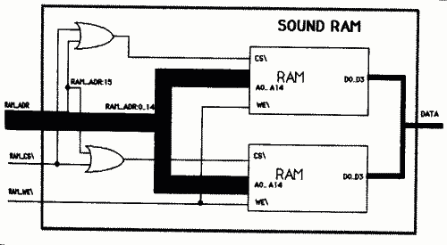
Here's where we actually physically kept the data. The only complicated stuff here stems from the fact that we had to use two chips to store the noise. We handled this by means of the high bit of RAM_ADR. Each RAM only had 15 address bits. The 16th bit of the address was used to select which chip to write/read to/from. The chip select of one ram received RAM_ADR:15 ORed with RAM_CS\. Thus both RAM_ADR:15 and RAM_CS\ would have to go low for that RAM's Chip Select to go active. The other RAM got the same input, with the very important adjustment that the inverse of RAM_ADR's high bit was used. Thus that chip would only be selected if RAM_CS\ went low and RAM_ADR:15 was high. Pretty slick, huh?
The other control input for the RAMs was RAM_WE\ which, like RAM_CS\, came from the controller. RAM_WE\ was hooked right up to the Write Enables of the RAMs. So the high bit of RAM_ADR and RAM_CS\ would decide if a chip was selected. RAM_ADR would choose which address to look up. RAM_WE\ would determine if the selected RAM was reading or writing.
Amazingly enough, the RAMs were connected to the Data Bus, which it could fetch data from, or shove data back, depending. Since our RAMs were capable of holding 8 bits, we considered trying to get by using just one RAM, and just using half a word at a time. When we figured out how much extra work would be involved - setting up a multiplexer to select which data lines to write to the data bus, decoders to decide which bits to write to from the bus, registers to store the bits which weren't changing... We think we found the more elegant solution.
In addition to the need to keep track of huge amounts of noise data, we wanted to keep track of a couple of 2-bit numbers:
So of course we worried a lot more about how to store the 2-bit numbers. We came up with more hare-brained schemes about these little jobbies... Until we figured out just how many controller input slots we had available. And outputs.
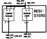
The system we ended up with was using 2 374 latches. These have input enable. The controller outputs MSG_MC\ (Write Message Count) and MSG_CM\ (Write Current Message) control these. If either goes low, the values the controller is outputting to MSG_WD0 and MSG_WD1 (Write Data 0, 1) get latched by the appropriate register. If both Write MC and Write CM go low, both will latch the data. Their outputs are sent back to the controller as MSG_CM0, 1, MSG_MC0, 1. The contents of Current Message are also fed into the Address Controller as ADR_DAT.
This system relies on a lot of work by the controller. It requires 4 controller outputs and a whopping four controller inputs. Other systems we considered included setting up a separate register bus. This would have involved using Tri-State® registers, so that more than one register output wouldn't end up on the bus at once. It would have meant that only two controller inputs would have been necessary - the controller could decide which it wanted to look at and set its control bit high. An adder set to add one to its input with a Tri-State® buffer between its output and the bus could be used to increment any register, a common operation. This was an okay system. Then we hit upon the idea of using a multiplexer to select between the registers instead of relying on Tri-State® buffers. We considered using an incrementer with this system, too. But again, it seemed that having more microcode would be simpler than wiring up the extra chip. However, if in the future we needed more controller inputs freed up, we would probably turn to this system.
If we wanted to minimize controller outputs, we would have used a counter to store both. Store Current Message in the low bits, Message Count in the high bits. To increment Current Message, increment the counter, and if this results in messing up Message Count, increment Message Count 3 times to get it back to its old level. To increment Message Count for whatever reason, increment 4 times. This would only require one controller output, but loads of microcode.
For our purposes, ours was a happy compromise.
This little baby was used to generate the beep with which SPAM serenades its users.
At all times the signal CLK_BEP is fed into this 3-state buffer. This signal changes at half the speaker's sampling speed. So when it ends up on the data bus it produces a nice tone or beep. When the controller signal BGN_BEP hits the buffer, The Beep Generator In All Its Glorious Splendor (known as "The Beep Generator In All Its Glorious Splendour" in the U.K.) does just that - admits CLK_BEP onto the bus.
Its output is the data bus.
The Beep Generator In All Its Glorious Splendor is such a miracle of elegance that we never really came up with any better way to wire it up, as our only real regret with it is that its name is larger than the physical chip.
Next: Microcode